- 您现在的位置:买卖IC网 > Sheet目录318 > CAT3604VHV4-GT2 (ON Semiconductor)IC LED DVR WHT CLR BACKLT 16TQFN
�� �
�
�CAT3604V�
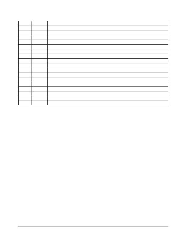
�Table� 6.� PIN� DESCRIPTION�
�Pin� #�
�1�
�2�
�3�
�4�
�5�
�6�
�7�
�8�
�9�
�10�
�11�
�12�
�13�
�14�
�15�
�16�
�TAB�
�Name�
�EN�
�NC�
�NC�
�NC�
�RSET�
�VOUT�
�VIN�
�C1+�
�C1� ?�
�C2� ?�
�C2+�
�GND�
�LED4�
�LED3�
�LED2�
�LED1�
�GND�
�Function�
�Device� enable� (active� high).�
�Not� connected� inside� the� package.�
�Not� connected� inside� the� package.�
�Not� connected� inside� the� package.�
�Connect� resistor� RSET� to� set� the� LED� current.�
�Charge� pump� output� connected� to� the� LED� anodes.�
�Charge� pump� input,� connect� to� battery� or� supply.�
�Bucket� capacitor� 1� Positive� terminal�
�Bucket� capacitor� 1� Negative� terminal�
�Bucket� capacitor� 2� Negative� terminal�
�Bucket� capacitor� 2� Positive� terminal�
�Ground� Reference�
�LED4� cathode� terminal.�
�LED3� cathode� terminal.�
�LED2� cathode� terminal.�
�LED1� cathode� terminal.�
�Connect� to� GND� on� the� PCB.�
�Pin� Function�
�VIN� is� the� supply� pin� for� the� charge� pump.� A� small� 1� m� F�
�ceramic� bypass� capacitor� is� required� between� the� VIN� pin�
�and� ground� near� the� device.� The� operating� input� voltage�
�range� is� from� 2.5� V� to� 5.5� V.� Whenever� the� input� supply� falls�
�below� the� under� ?� voltage� threshold� (1.8� V),� all� the� LED�
�channels� are� disabled� and� the� device� enters� shutdown� mode.�
�EN� is� the� enable� input� and� the� high� resolution� PWM�
�dimming� control.� Levels� of� logic� high� and� logic� low� are� set�
�at� 1.3� V� and� 0.4� V� respectively.� When� EN� is� initially� taken�
�high,� the� device� becomes� enabled� and� all� LED� currents� are�
�set� according� to� the� R� SET� resistor.� To� place� the� device� into�
�“zero� current”� shutdown� mode,� the� EN� pin� must� be� held� low�
�for� at� least� 1.5� ms.�
�VOUT� is� the� charge� pump� output� that� is� connected� to� the�
�LED� anodes.� A� small� 1� m� F� ceramic� bypass� capacitor� is�
�required� between� the� V� OUT� pin� and� ground� near� the� device.�
�GND� is� the� ground� reference� for� the� charge� pump.� The� pin�
�must� be� connected� to� the� ground� plane� on� the� PCB.�
�C1+,� C1� ?� are� connected� to� each� side� of� the� ceramic� bucket�
�capacitor� C� 1� .�
�C2+,� C2� ?� are� connected� to� each� side� of� the� ceramic� bucket�
�capacitor� C� 2� .�
�LED1� to� LED4� provide� the� internal� regulated� current�
�source� for� each� of� the� LED� cathodes.� These� pins� enter�
�high� ?� impedance� zero� current� state� whenever� the� device� is�
�placed� in� shutdown� mode.� If� an� LED� pin� is� directly� tied� to�
�VOUT,� that� channel� is� disabled.�
�TAB� is� the� exposed� pad� underneath� the� package.� For� best�
�thermal� performance,� the� tab� should� be� soldered� to� the� PCB�
�and� connected� to� the� ground� plane.�
�RSET� is� connected� to� the� resistor� (R� SET� )� to� set� the� current�
�for� the� LEDs.� The� voltage� at� this� pin� regulated� to� 0.6� V.� The�
�ground� side� of� the� external� resistor� should� be� star� connected�
�back� to� the� GND� of� the� PCB.� In� shutdown� mode,� RSET�
�becomes� high� impedance.�
�http://onsemi.com�
�9�
�发布紧急采购,3分钟左右您将得到回复。
相关PDF资料
CAT3606HV4-T2
IC LED DRVR WHITE BCKLGT 16-TQFN
CAT3614HV2-T2
IC LED DRVR WHITE BCKLGT 12-TDFN
CAT3616HV4-GT2
IC LED DRVR WHITE BCKLGT 16-TQFN
CAT3636HV3-GT2
IC LED DVR 6CH QUAD MODE 16TQFN
CAT3643HV2-T2
IC LED DRVR WHITE BCKLGT 12-TDFN
CAT3644HV3-GT2
IC LED DVR 4CH QUAD MODE 16TQFN
CAT3647HV3-GT2
IC LED DRVR WHITE BCKLGT 16-TQFN
CAT3648HV3-GT2
IC LED DRVR WHITE BCKLGT 16-TQFN
相关代理商/技术参数
CAT3604VHV4-T2
制造商:CATALYST 制造商全称:Catalyst Semiconductor 功能描述:4-Channel Quad-Mode⑩ LED Driver with Open/Short LED Detection
CAT3604VHV9-A3
制造商:Rochester Electronics LLC 功能描述: 制造商:Catalyst Semiconductor 功能描述:
CAT3606
制造商:ONSEMI 制造商全称:ON Semiconductor 功能描述:6-Channel Low Noise Charge Pump White LED Driver
CAT3606_08
制造商:CATALYST 制造商全称:Catalyst Semiconductor 功能描述:6-Channel Low Noise Charge Pump White LED Driver
CAT3606HS4
制造商:CATALYST 制造商全称:Catalyst Semiconductor 功能描述:6-Channel Low Noise Charge Pump White LED Driver
CAT3606HV4
制造商:CATALYST 制造商全称:Catalyst Semiconductor 功能描述:6-Channel Low Noise Charge Pump White LED Driver
CAT3606HV4-GT2
制造商:ONSEMI 制造商全称:ON Semiconductor 功能描述:6-Channel Low Noise Charge Pump White LED Driver
CAT3606HV4-T2
功能描述:LED照明驱动器 Lo-Noise Charge Pump White LED RoHS:否 制造商:STMicroelectronics 输入电压:11.5 V to 23 V 工作频率: 最大电源电流:1.7 mA 输出电流: 最大工作温度: 安装风格:SMD/SMT 封装 / 箱体:SO-16N